Low Cost Semiconductor Reliability Testing
We now offer a full range of Reliability Testing Services for our Semiconductor clients with a unique cost saving approach
Semiconductor Reliability Testing Services – with our unique cost saving advantage
NanoScope offers turnkey reliability testing services for our Semiconductor clients from our facility in Bristol, UK. We have teamed up with our 2 partners to offer an extended range of services with some innovative ways to reduce your testing costs. Here’s some example services and how we can maximise your budget.
MSL Evaluation
This identifies the classification level of non-hermetically sealed surface mounted solid-state devices, which may be sensitive to moisture induced stress. A package’s MSL sets the parameters for subsequent device preconditioning. The basic test sequence is shown below and assumes that pre and post electrical tests are conducted at the customer site. The test is performed to IPC/JEDEC Standard J-STD-020D.1
- Initial Visual Inspection
- 1st Acoustical Microscope (CSAM)
- Initial Bake – 24 hrs @ 125°C
- Moisture Soak – Temp/Humidity at required level
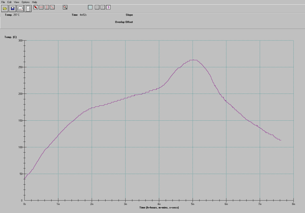
- Reflow (IR bake) x3 @260°C
- Final Visual Inspection
- 2nd Acoustical Microscope (CSAM)
- Optional written report
Device Pre-conditioning
This exposes a batch of devices to the upper limit of the MSL level specified prior to that batch undergoing reliability testing. Pre-conditioning may use all of the sequence shown above, but is often steps 3, 4, and 5 only. The accelerated equivalent tests are also available. Pre-conditioning is available for the full range of MSL’s and is performed to JEDEC Standard JESD22-A113
Reliability Services Certified Services
NanoScope is the first RELIABILITY testing lab to offer both CERTIFIED and UN-CERTIFIED testing options (lower cost) . Many R&D activities do not require certification, examples could include – testing new packages, solder paste experiments, moisture sensitivity on new materials, evaluating your testing protocol (THB or HAST), supplier component quality checks (pre-assembly), solder reflow experiments…
Some regular testing protocols are available with both options include
PRECON – Device pre-conditioning (prior to package tests) JESD22-A113
MSL – Moisture Sensitivity Level (levels 1,2 and 3)
THB – Temperature & Humidity
HASTEST (unbiased UHAST) – Highly Accelerated Stress Test to JESD22-A118
No drop in QUALITY – All testing is done to the specified JEDEC STANDARD and observing industry best practice, documented calibration and reporting, but with the flexibility of lower cost testing for R&D device lots.


INTRODUCING our reliability partners Reltech and Rood Microtec
For a full turnkey service with even better savings, we have teamed up with our close collaborators RELTECH Ltd and ROOD MICROTEC Gmbh to offer a complete portfolio of both FULLY CERTIFIED and UN-CERTIFIED (lower cost) semiconductor reliability testing.
For customers booking a program of tests with NanoScope we can offer the seamless total solution provision of any combination of testing using the combined resources of 3 Laboratories, while also reducing total costs with our unique tailored approach. Email us here for more information.
The list below is just a SELECTION of the total capabilities available to you.
All projects are completed to JEDEC Standard JESD47.
Device Qualification Tests
- High Temperature Operating Life (HTOL) JESD22-A108/JESD85
- Early Life Failure Rate (ELFR) JESD22-A108/JESD74
- Low Temperature Operating Life (LTOL) JESD22-A108
- High Temperature Storage Life (HTSL) JESD22-A103
Non-Hermetic Package Qualification Tests
- High Temperature Storage (HTS) JESD22-A103 & A113
- Temperature Humidity Bias (THB) JESD22-A101
- Biased Highly Accelerated Temperature & Humidity Stress (HAST) JESD22-A110
- Temperature Cycling (TC) JESD22-A104
Don't Be Shy. Get In Touch.
If you are interested in working together, send us an inquiry and we will get back to you straight away.
Circuit Nano-Surgery and Failure Analysis Online Tutorial
NanoScope gave an Online invited Tutorial on behalf of IMAPS UK on the 18th September on the subject of Focused Ion Beam (FIB) Circuit Nano-Surgery and Failure Analysis from Board to Gate.
E-Newsletter Summer 2019
Here are some examples of our new services, and how they complement our existing imaging and non-destructive analysis. There is a quick guide to the specific advantages of each technique to show how your FA, NPI or development project can benefit.
E-Newsletter Spring 2014
IC Decap, MEMS Gel coat removal and through WL-CSP modification capabilities available now


