Failure Analysis Service
Advanced Microscopy enabled FA services for Semiconductor clients across UK & Europe
Failure Analysis /Quality Engineers
Based around our advanced Microscopy and FIB expertise, NanoScope offer a suite of fast turn Failure Analysis services for our semiconductor clients.
Each analysis can be specified for 3 levels of detail, depending on your time-line for resolving the issue and budgetary requirements.
- Basic – an initial investigation to check specifically defined elements are in order.
- Intermediate – a more in depth investigation checking the specifics of the product in line with the specifications stated.
- Detailed – a more involved investigation to identify the route cause of a specific problem which may involve a more iterative approach and more detailed consultation.
We are happy to offer cost-free initial consultancy for selecting which procedures and techniques are the most applicable for solving your issue the most efficiently.
Services offered
- External optical examination
- Build a test socket board
- Basic benchtop electrical testing
- X-ray package analysis
- CSAM package analysis
- Decapsulation
- Internal optical inspection
- Anti-counterfeit check (structure/features)
- High resolution Thermal Imaging
- FIB/FEG-SEM internal inspection
- In-circuit electrical micro-probing (inc. to FIB probe pads)
- FIB Sectioning and imaging (w/wo iterative slicing)
- Process Metrology (inc. SI/SE imaging)
- SEM EDS studies
- FIBxTEM Sectioning
- TEM imaging analysis (TEM/STEM) – BF/DF
- TEM X-ray or EELS elemental analysis
- Written report
Based on your description of the issue identified, we will propose a workflow with a level of detail and a cost for the analysis process prior to starting the project. Should additional investigative work be required during the analysis this can be easily added at the time.

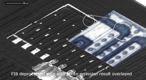
EMMI fault finding with metal layers removed by FIB.

Non-destructive X-ray analysis of packaged parts.

Adding probe pads to any node for electrical debug.
Don't Be Shy. Get In Touch.
If you are interested in working together, send us an inquiry and we will get back to you straight away.
Merry Christmas 2023 – It’s been a Quality Year adding these exciting new Capabilities
Our big company NEWS is that we are now ISO 9001:2015 Certified
Our NEW microscope this year is a Sonoscan D24 Acoustic Microscope (large area CSAM).
Our New Technique this year is our Plasma FIB Capability.
We now offer ThermoFisher Hydra capabilities to our customers now including.
Lastly our new Sample Preparation Technique is Mechanical Grinding and Polishing.
Circuit Nano-Surgery and Failure Analysis Online Tutorial
NanoScope gave an Online invited Tutorial on behalf of IMAPS UK on the 18th September on the subject of Focused Ion Beam (FIB) Circuit Nano-Surgery and Failure Analysis from Board to Gate.
read moreWe are OPEN.
We are still open, but with a few sample handling improvements
read more


