
FIB Services for Failure Analysts and Product Test Engineers
Electrical Micro-Probing – also to FIB deposited pads connected to buried nodes
Electrical micro-probing permits the driving or monitoring of a voltage or signal at any mid-circuit node(s) with or without available probe pads.
Our micro-probing facility with optical microscope permits direct electrical connection to structures down to 10×10 microns. This is sufficient to connect to power structures and any nodes connected to FIB deposited probe pads in a device.
We have a number of different probe types available or customers can repeat their own tips setup and test condition. Power supplies and a Tektronix curve tracer are on-site and available for your use to support your test protocol and confirm your FIB-layout edits and functionality changes are successful.
For a detailed description of the equipment and techniques available, go to the Tools and Techniques page.
There are 3 clear advantages
- It can be QUICK as it can be done directly on opened circuits without changing the device layout.
- IT WORKS ON PASSIVATED TOP LAYER TRACKS – by using FIB to open windows in the passivation coating.
- IT WORKS ON BURIED NODES –by first depositing a FIB probe pad on top of the passivation and connecting it down to the target node.


Don't be shy, get in touch.
If you are not sure about an aspect of this technique we’re happy to chat through it with you.

E-Newsletter Summer 2019
Here are some examples of our new services, and how they complement our existing imaging and non-destructive analysis. There is a quick guide to the specific advantages of each technique to show how your FA, NPI or development project can benefit.
read moreA Very Merry FIB-mas from NanoScope
read more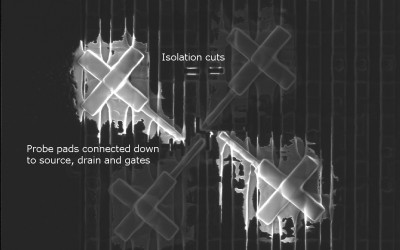
FIB assisted electrical debug for 1st Silicon
An often overlooked option in the race to get 1st Silicon devices working, is simple electrical probing (μm), but why is this?
read more